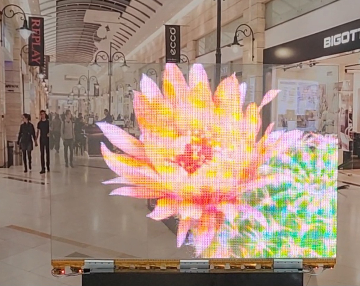
Glass is ideal for transparent digital signage due to its translucency and thermal conductivity.
Traditional methods for conductive traces, like etching, sputtering, and silver inks, are costly, energy-intensive, and environmentally damaging.
Copprint’s copper ink solution offers a cost-effective, eco-friendly alternative, printing ultra-thin, high-translucency traces directly onto glass, transforming transparent display technologies.
Simply Print Any Conductive Trace
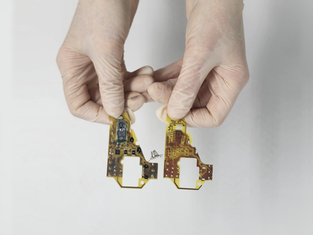
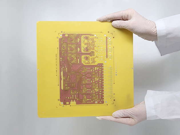
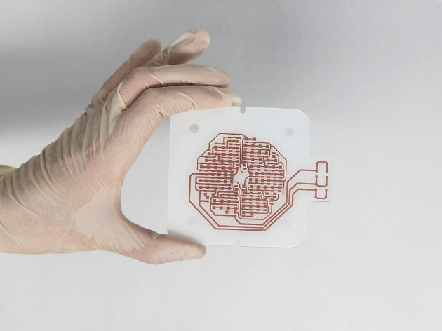
Copprint’s additive copper technology enables faster prototyping and the creation of highly customized PCB designs that are challenging or impossible with traditional chemical etching.
With Copprint Nano Copper inks, you can print any conductive trace on a wide range of rigid (FR4, CEM3, Aluminum, Glass) and flexible (PET, PI, Paper, Biodegradable) substrates, offering unparalleled design flexibility.
50% Lower PCB Manufacturing Costs
Copprint copper inks enable the shift from traditional chemical etching to additive copper manufacturing, reducing PCB fabrication costs by 40-55%.
Printed copper eliminates the need for costly and toxic chemical etching processes, including copper sheet waste, CU laminates, and the high energy and environmental costs associated with plating (PTH), photolithography, and stripping/etching.
50% Reduction in Carbon Emissions per PCB
Copprint inks are eco-friendly, made from recycled, compostable copper, reducing CO2 emissions by cutting material waste, energy consumption, and additional processing.
Additive copper manufacturing lowers pollutants and toxins, enabling cleaner, onshore production anywhere.
Onshoring with additive manufacturing reduces transportation emissions—especially as 90% of traditional PCB production occurs in APAC. It also offers better supply chain control, faster fulfilment, lower shipping costs, and enhanced IP protection.