
Charles Ducas patent drawing
The acronym PCB stands for Printed Circuit Board, but PCBs aren’t actually “printed” — they’re chemically etched. So, why do we still call them PCBs?
The concept of printed conductive traces dates back a century. In 1925, Charles Ducas patented the idea of “printed wire” to create electrical paths on an insulated surface. His concept involved printing conductive ink onto an insulated substrate, marking a significant departure from traditional point-to-point wiring. Ducas’ patent laid the foundation for the development of printed circuits (PCBs). However, it wasn’t until the 1930s that Paul Eisler created the first operational PCB. Eisler’s circuit used Ducas’ idea of printed wire to form a simple radio system. Initially, the first implementations used silver inks, although the patent also mentioned printed copper. However, copper ink was not available at that time.
The next major evolution of PCBs came during World War II, with the large-scale production of proximity fuses—game-changing devices used in artillery and anti-aircraft weaponry. These circuits needed to be robust enough to withstand the shock and vibration of being fired from a gun, while maintaining functionality. To meet this challenge, specialized materials and construction techniques were employed. Ceramic plates were screen-printed with metallic paste for conductors and carbon material for resistors, while ceramic disc capacitors and subminiature vacuum tubes were soldered in place. The U.S. military produced nearly 10 million fuses between 1943 and 1944, each containing around 130 miniaturized electronic components. The total cost of this effort would amount to over $15 billion in today’s U.S. dollars.
For a contemporary review, see: New Advances in Printed Circuits,
Brunetti, Cledo (22 November 1948). Washington, DC: National Bureau of Standards.
By the 1950s, PCB manufacturing shifted to chemical etching—a subtractive manufacturing process used to create patterns or features on a material surface, typically a copper or aluminum semiconductor substrate. This process involves using a chemical solution, called an etchant, to selectively remove material from the surface, leaving behind a desired conductive pattern or feature. The adoption of chemical etching allowed for faster, more accurate production and facilitated the miniaturization of electronic devices. Today, chemical etching remains the standard method in a $75 billion PCB manufacturing market.

Brunetti, Cledo (22 November 1948). New Advances in Printed Circuits. Washington DC: National Bureau of Standards.
While chemical etching is widely used in PCB manufacturing, it presents significant environmental, cost, and design challenges:
Copprint Additive Copper Manufacturing is bringing printing back into PCB production. Our copper inks provide high conductivity, are environmentally friendly, and support clean, onshore manufacturing. With a lower-cost, high-precision process, we offer full substrate flexibility, enabling the simple printing of even the most complex PCB designs. Copprint is making PCBs great again!
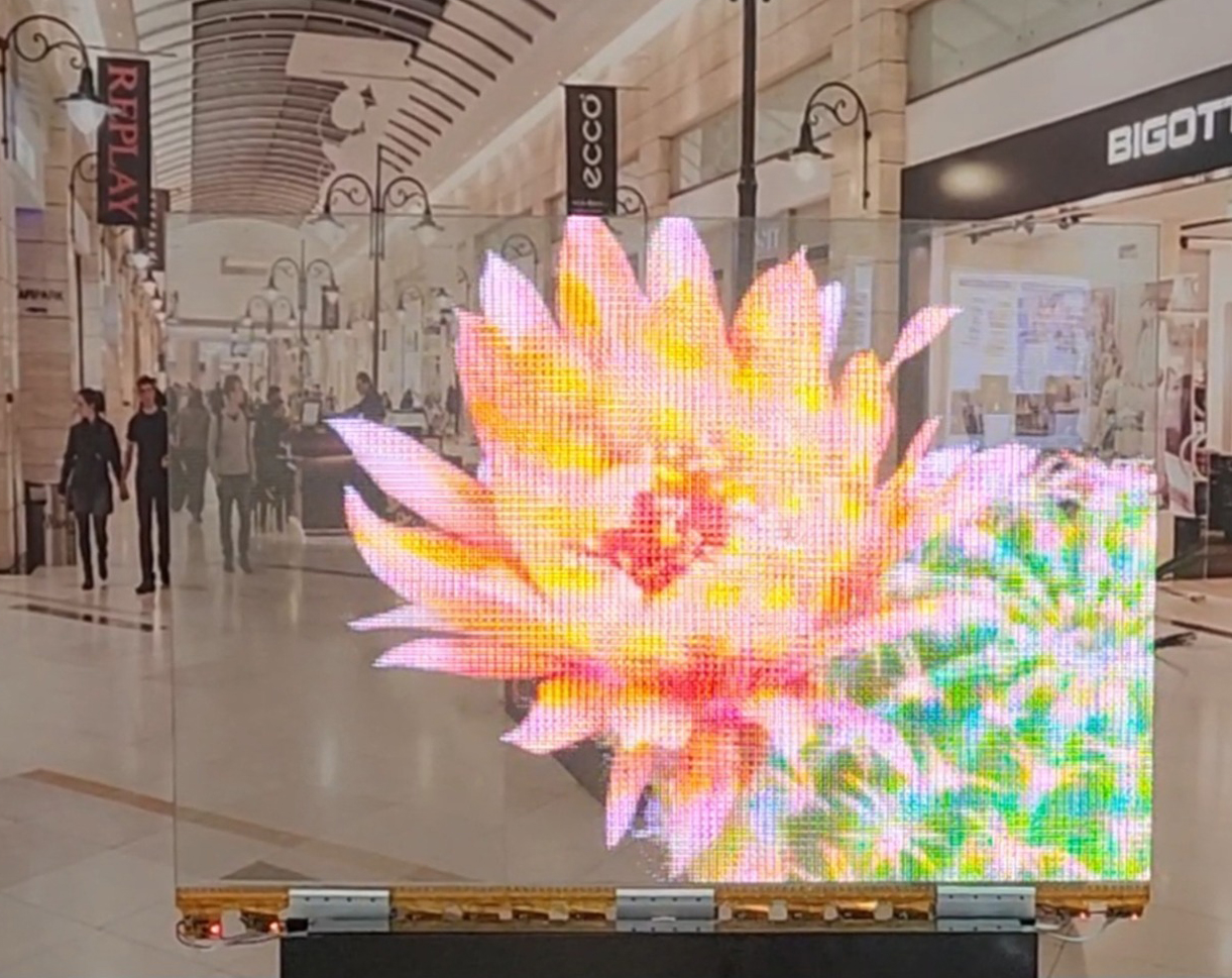
Glass is ideal for transparent digital signage due to its translucency and thermal conductivity. Traditional methods for conductive traces, like...

We are excited to be exhibiting Copprint sustainable additive electronic at LOPEC 2024.

Copprint has been nominated by the Cleantech 100 as a leading changemaker in the Materials & Chemicals category.
